
Toward AI-Enabled Silicon Photonics Design
How X’s moonshot for AI invention could unlock the future of data centers
Last week at the Optical Fiber Communication Conference in San Diego, my team presented the results of our work to design a high performance, compact CWDM-4 demultiplexer – commonly referred to as a “demux.” We shared how our AI for photonics design platform — drawing on tools and techniques from the worlds of inverse design, simulation, topology optimization, and machine learning — can generate high performance results in simulation and replicate them in the real world. We’ve demonstrated this with a leading semiconductor foundry, a critical step toward data center-ready integrated demux devices. If you're curious to dive deeper on the technical details check out our paper here.
The communication bandwidth bottleneck
We believe this work is coming at a critical time for AI infrastructure. As the world’s demand for AI applications has accelerated in recent years, compute power in data centers has advanced exponentially, but communication bandwidth has not kept pace. This communications bottleneck isn’t just limiting the flow of information within and between data centers; it’s rate limiting humanity’s potential to harness the beneficial potential of artificial intelligence — from discovering new drugs faster, to finding new ways to help with climate change.
Engineers designing data center systems to meet the emerging needs of AI applications are exploring many strategies to enable more information to be moved between processing units at smaller and smaller scales. One widely used tool is wavelength division multiplexing, or WDM. WDM involves simultaneously sending datastreams from lasers of varied wavelengths on the same optic fiber. This enables more information to be transmitted at once than an optical fiber carrying a single wavelength.
At the receiver end of that WDM fiber channel, a device known as demultiplexer, or “demux”, is used to separate information back into multiple datastreams.The current solution for demuxing is a separately packaged device that utilizes conventional optics approaches. We believe that such devices are inadequate for the emerging needs of AI applications due to their large size, high cost, and system complexity implications.
Integrated silicon photonics — which involves creating lightguides and other optical features directly in silicon chips — has long been considered a promising way to remove these barriers and help address the communications bandwidth challenge. Light can carry far more information than copper, but designing compact, efficient devices that control light is fiendishly hard. Today it takes teams of highly skilled engineers multiple months to create new designs, and many expensive, time-consuming production cycles for foundries to make and test, rework, and eventually validate these designs. A high-performance integrated demux is a very challenging specific need for which many approaches have been proposed, but none have been adopted at scale.
Tiny, integrated photonics systems that no human would invent
For the last few years we have been directing our efforts towards creating an AI photonics platform to generate high performance, compact, low cost designs that work within industry processes. We focused initially on developing a silicon-integrated CWDM-4 demux because it promises to be a missing link in data center communications technology.
Using our AI photonics design system as a creative collaborator, we can continuously generate novel and unintuitive designs. In the figure below, you can see a typical human designed integrated demux on the left and X’s demux on the right.
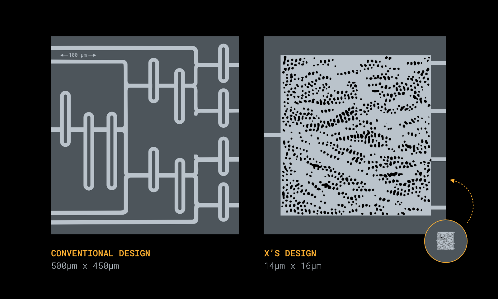
The one on the left looks rational and logical. It adheres to known practices and is planned according to human design principles and a human understanding of physics. The AI generated demux doesn’t – in appearance, it’s freeform, calling to mind patterns from nature. It meets all of the performance benchmarks we set and the foundry rules for production; however, it does this by interacting with light with strategies that are quite different from those used in conventional designs. While both devices are patterned directly onto a silicon photonic integrated circuit, the X AI designed demux is 1/1000th of the size of the human-designed example shown here. It also performs well repeatedly in the real world.
These results lead us to believe that we’re at a turning point where we’ll be able to design high performance devices of sizes that enable unprecedented levels of integration density, approaching the lower size limits of what physics allows with mass production materials. No longer limited by human practices and intuition, we believe the future of AI infrastructure will be driven by tiny, integrated photonics systems that no human would invent – unlocking previously inaccessible worlds of design.
This is just a first step: we're continuing to push the performance of demux devices, and also developing high performance designs for other key components and systems needed for the future of AI and other application spaces. If you're developing or deploying integrated photonics devices and are interested in exploring how these design capabilities might accelerate your development, please get in touch!